CST MWS微帶線仿真時候的疑問?
請教一下,微帶線仿真時,可以使用open 作為邊界條件么?
我使用open邊界條件時,發現S12在低頻處出現明顯損耗,求解原因。


可以。
我又來算命了:樓主你能確定端口模式是正確的嗎?
我又運行了一些模型,結果還是這樣子。
hefang老大 ,幫忙看下,模型里面哪個地方有問題啊!
仿真使用的模型:
http://pan.baidu.com/s/1dDEW8jJ
這次先說結論吧。CST只建議在仿真遠場屬性的時候才使用open (add space)邊界,如果只是觀察S參數的話應該盡量使用閉合邊界。不過,這并不表示仿真微帶線不可以使用開放邊界。唯一需要注意的是波導端口被建立在邊界內部的時候被稱為internal port,在絕大多數情況下這種波導端口必須添加shielding才能得到“正確”的結果。
樓主的模型:
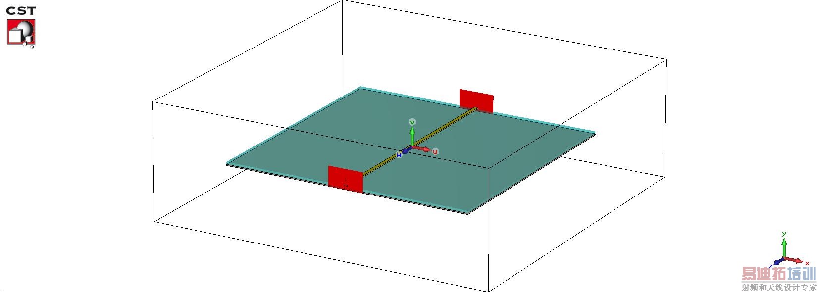
open邊界,6個方向設置了2的surrounding space。
使用新的網格模式,只設置一個對稱面,其余不做任何修改,得到的S參數:

S21:
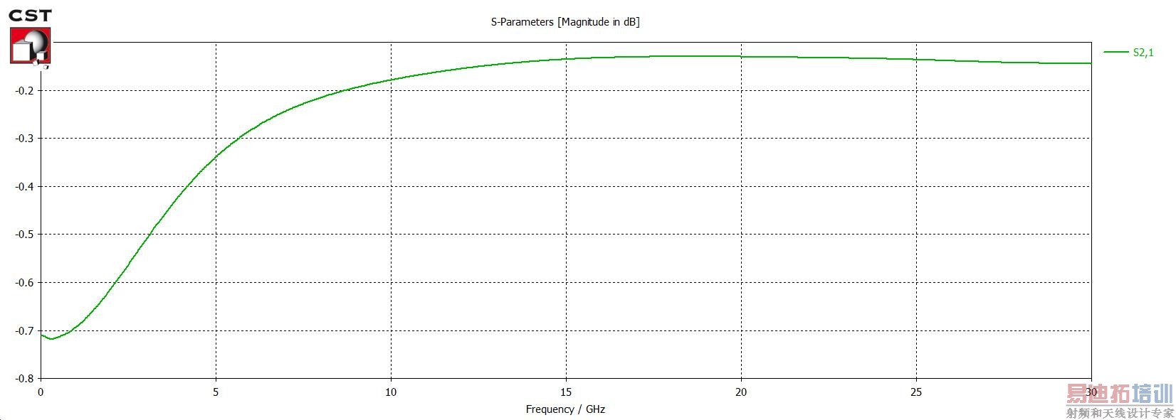
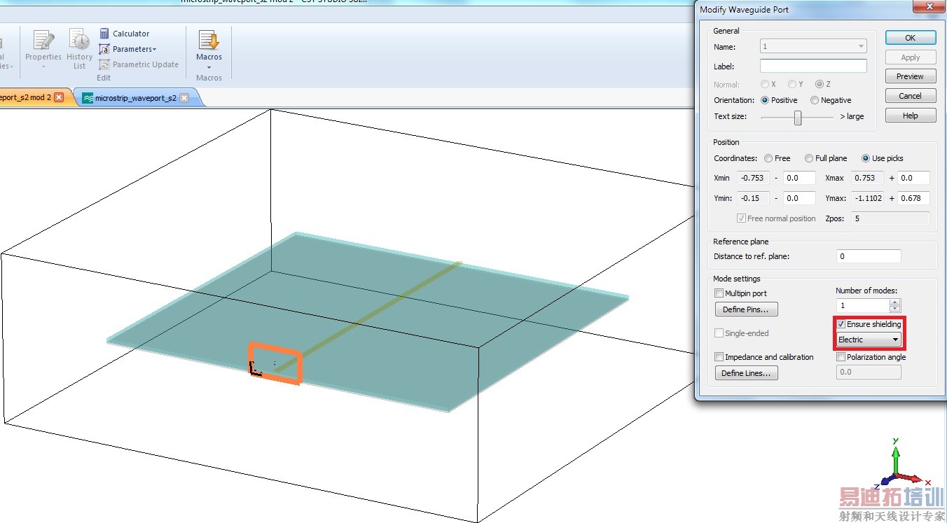
S21的情況和樓主類似。原因就是internal port在0頻不能正確工作。給兩個端口都添加Electric shielding:
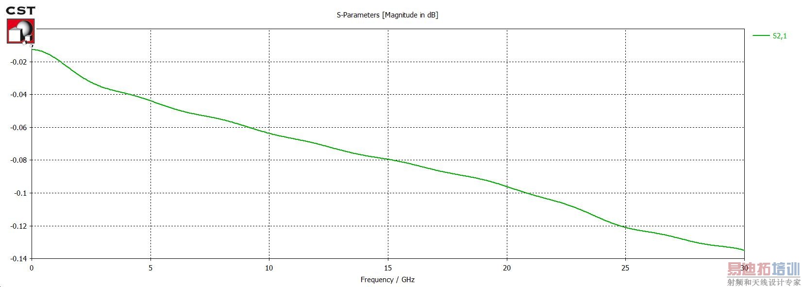
得到的S參數:

可以看到S11在0頻處比原先低了將近40 dB。可想而知S21也肯定有改善:
假設使用閉合邊界會怎樣呢?把邊界條件設置為conducting wall,取消surrounding space:

波導端口不需要electricl shielding,得到的S參數:
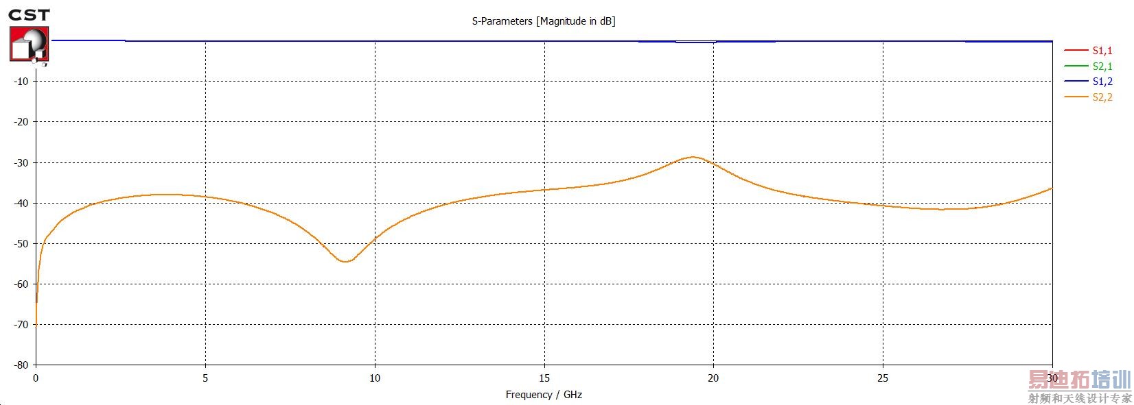
0頻處和上面一致,接近20 GHz出現諧振。S21:
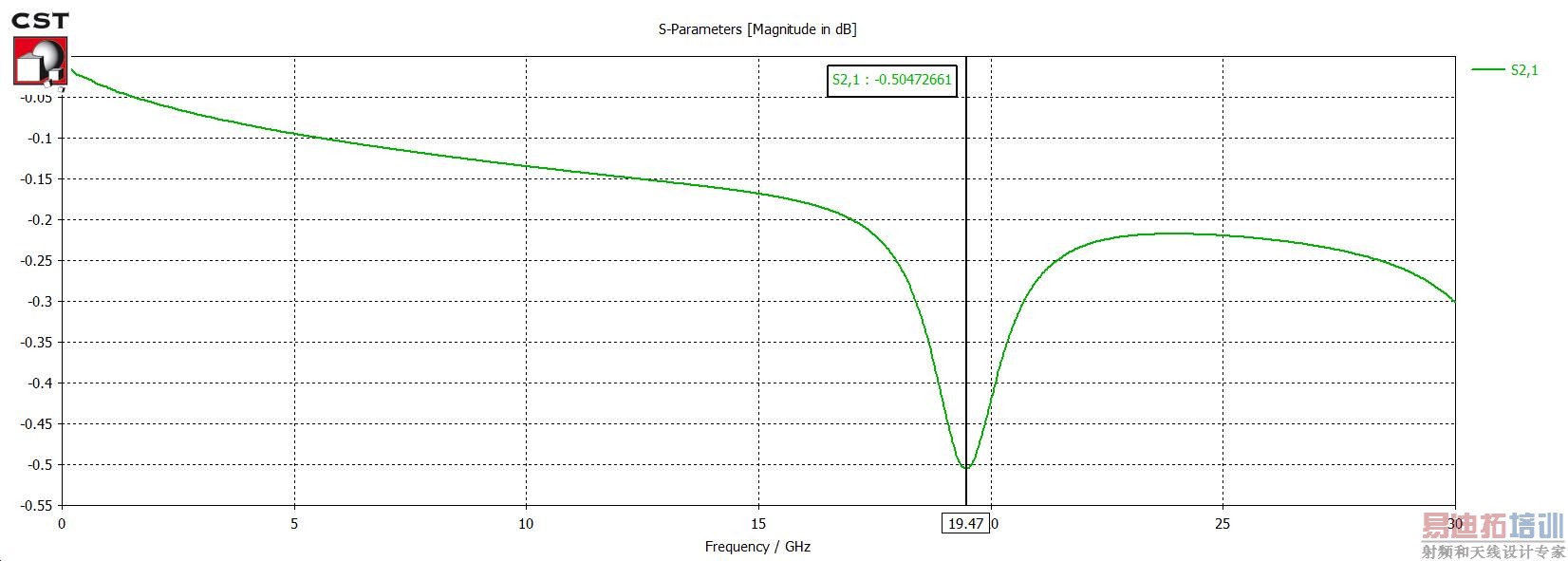
低頻處沒有樓主的問題。樓主可以自行計算閉合邊界是否在19.47 GHz處引發了腔體諧振(box resonance)。
結論:仿真非遠場問題盡量使用閉合邊界。如果一定要用開放邊界,內部波導端口需要設置電/磁屏蔽。
CST MWS幫助文件《Waveguide Port Overview》:
Ensure shielding
Especially for inner waveguide ports is important to apply an electric or magnetic shielding to ensure a consistent integration of the waveguide boundary into the calculation domain. In case of a hexahedral mesh, port shieldings are modeled as a tube in direction of field imprint, with a length of two grid cells. For tetrahedral meshes this extrusion is not necessary. Please not that the boundary condition can be influenced by a port shielding. Also, conductors might be short-circuited by an electric shield. Generally, a electric boundary condition or PEC materialis given higher priority compared to a magnetic shielding. Furthermore, the solver detects whether the port contains an outer region (as in the corners of a coaxial line). If this is the case, shielding the port will not have any effect and is therefore not applied.
CST MWS幫助文件《Waveguide Port》:
Ensure shielding: If the port mode domain is not already electrically shielded (as e.g. in a coaxial waveguide) this box can be checked to activate a special treatment of the boundary:electric: the boundary of the waveguide port is treated as a PEC shielding frame.
magnetic: the boundary of the waveguide port is treated as a PMC shielding frame. Note that conductors in the port shield will not be removed and might cut through the PMC shield.Leaving this box unchecked will apply the default treatment for port boundaries of the used solver.
CST MWS幫助文件《Special Solver Parameters - General》:
Ensure shielding for all ports: If this check button is enabled, a shielding frame of PEC or PMC type surrounding each waveguide port region will be added. This option causes higher reflections at ports. Therefore, it should only be used if a calculation has become unstable. Note that this setting will be ignored for already electrically shielded waveguides (e.g. coaxial waveguides). Leave this button unchecked to apply the default treatment for waveguide port boundaries.
收兵回營!
學習多謝hefang大大。