關于高速CAN總線的PCB layout要點
英文為文檔中的原文。

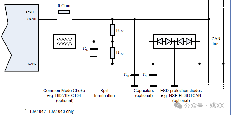
1、When a common mode choke is used, it should be placed close to the transceiver bus pins CANH and CANL
如果節點有共模電感,共模電感應該靠近收發器放置
2、The PCB tracks for the bus signals CANH and CANL should be routed close together in a symmetrical way. Its length should not exceed 10cm.
PCB板上的CANH和CANL走線時應該等長走線,緊耦合,相互靠近;且板上的走線不要超過10cm。
3、Avoid routing other “off-board” signal lines parallel to the CANH/CANL lines on the PCB due to potential “single ended” noise injection into CAN wires
如果PCB上某類走線最終會通過連接器引出到板外,那么在PCB上,CANH和CANL就不要平行于這類走線。
4、The ESD protection should be connected close to the ECU connector bus terminals
ESD器件靠近ECU的連接器端子放置。
5、Place VCC and VIO capacitor close to transceiver pin.
退耦電容靠近收發器的PIN放置。
6、For TJA1051/3 and TJA1042/3: Decouple the VIO pin by a capacitor to VCC (instead GND) close to the transceiver pin to achieve a high-frequent short of the supplies and thus to improve the electromagnetic immunity by enabling the same HF-conditions like existing with VCC connected directly to VIO in 5V-only environments.

對于有VIO引腳的收發器,如果VCC和VIO是不同的電壓,那么它們之間的的耦合電容(圖中已標出)應該盡可能的靠近收發器,以實現VCC和VIO之間的高頻通路。如果VCC和VIO是同一個電壓,VCC和VIO直接連接。
7、The track length between communication controller / μC and transceiver should be as short as possible
CAN的控制器(通常在處理器內部,少部分是獨立的)與收發器之間的走線應該盡可能的短。
8、The ground impedance between communication controller (μC) and transceiver should be as low as possible
CAN的控制器的“地”與收發器的“地”的互連應該盡可能的低阻,建議采用完整地平面連接。
9、Avoid applying filter elements into the GND signal of the μC or the Transceiver. GND has to be the same for Transceiver and μC.
CAN的控制器的“地”與收發器的“地”是同一個地,它們之間不要加濾波元件(典型的如磁珠等等)。也不要做成單點互連的形式。
這一條其實和第8條表達的意思本質上相同的。


